- 您现在的位置:买卖IC网 > Sheet目录477 > MICRF506DEV1 (Micrel Inc)EVAL BOARD EXPERIMENTAL MICRF506
Micrel
MICRF506BML/YML
The lengths of the N, M, and A registers are 12, 12
and 6 respectively The values can be calculated
from the following formula:
C L =
1
C 10
1
+
1
C 11
+ C parasitic
The parasitic
capacitance
is the
pin input
= XCO =
f VCO f RF × 2
( 16 × N + A ) × 2 ( 16 × N + A )
f PhD
where
f
M
M ≠ 0
1 ≤ A<N
=
capacitance and PCB stray capacitance. Typically,
the total parasitic capacitance is around 6pF. For
instance, for a 9pF load crystal the recommended
values of the external load capacitors are 5.6pF.
It is also possible to tune the crystal oscillator
internally by switching in internal capacitance using
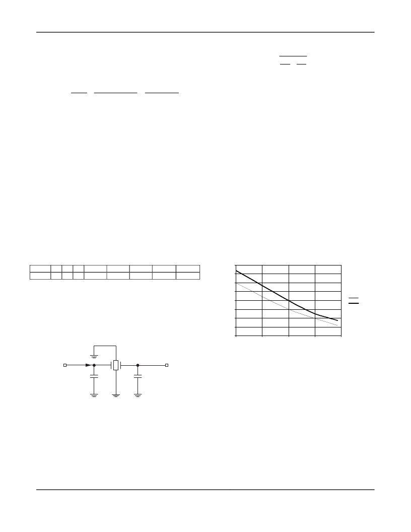
5 tune bits XCOtune4 – XCOtun0. When XCOtune4
f PhD : Phase detector comparison frequency
f XCO : Crystal oscillator frequency
f VCO : Voltage controlled oscillator frequency
f RF : RF carrier frequency
There are two sets of each of the divide factors (i.e.
A0 and A1). If modulation by using the dividers is
selected (that is Modulation1=1, Modulation0=0), the
two sets should be programmed to give two RF
frequencies, separated by two times the specified
frequency deviation. For all other modulation
methods, and also in receive mode, the 0-set will be
used.
– XCOtune0 = 0 no internal capacitors are
connected to the crystal pins. When XCOtune4 –
XCOtune0 = 1 all of the internal capacitors are
connected to the crystal pins. Figure 6 shows the
tuning range for two different capacitor values, 1.5pF
and no capacitors.
The crystal used is a TN4-26011 from Toyocom.
Specification: Package TSX-10A, Nominal frequency
16.000000 MHz, frequency tolerance ±10ppm,
frequency stability ±9ppm, load capacitance 9pF,
pulling sensitivity 15ppm/pF. When the external
capacitors are set to 1.5pF and the XCOtune=16,
the total capacitance will normally be ~9pF.
Crystal Oscillator (XCO)
Adr D7 D6 D5 D4
D3
D2
D1
D0
100,0
0001001
‘0’
‘0’
‘1’
XCOtune4 XCOtune3 XCOtune2
XCOtune1
XCOtune0
80,0
60,0
The crystal oscillator is a very critical block. As the
crystal oscillator is a reference for the RF output
frequency and also for the LO frequency in the
receiver, very good phase and frequency stability is
40,0
20,0
0,0
-20,0
2x1.5pF
2x0pF
required. The schematic of the crystal oscillator’s
external components for 16MHz are shown in Figure
5.
-40,0
-60,0
0
8
16
24
32
XCO bitvalue
Pin 24
Y1
Pin 23
XTALOUT
C10
5.6pF
TSX-10A
C11
5.6pF
XTALIN
Figure 6. XCO Tuning
The start up time is given in Table 7. As can be
seen, more capacitance will slow down the start up
time.
Figure 5. Crystal Oscillator Circuit
The crystal should be connected between pins
XTALIN and XTALOUT (pin 23 and 24). In addition,
loading capacitors for the crystal are required. The
loading capacitor values depend on the total load
capacitance, C L , specified for the crystal. The load
capacitance seen between the crystal terminals
should be equal to C L for the crystal to oscillate at
the specified frequency.
The start-up time of a crystal oscillator is typically
around a millisecond. Therefore, to save current
consumption, the XCO is turned on before any other
circuit block. During start-up the XCO amplitude will
eventually reach a sufficient level to trigger the M-
counter. After counting 2 M-counter output pulses
the rest of the circuit will be turned on. The current
consumption during the prestart period is
approximately 280 μ A.
July 2006
16
M9999-092904
+1 408-944-0800
发布紧急采购,3分钟左右您将得到回复。
相关PDF资料
MICRF507YML TR
TXRX FSK LOW PWR W/AMP 32MLF
MICRF600DEV1
KIT DEV RADIOWIRE 902-928MHZ
MK01-C
SENSOR REED SPST-NO SMD
MK01-H
SENSOR REED SPDT-CHANGE SMD
MK02/0-1A66-500W
SENSOR REED SPST-NO
MK02/6-0
SENSOR REED PCB 24MM T/H
MK03-1C90C-500W
SENSOR REED SPDT CYLINDER
MK05-1A66C-500W
SENSOR REED SPST-NO SCREW MOUNT
相关代理商/技术参数
MICRF506DEV1
制造商:Micrel Inc 功能描述:KIT MICRF506 EVALUATION
MICRF506YML
制造商:Micrel Inc 功能描述:410/450MHZ ITRANSCEIVER SMD MLF32 制造商:Micrel Inc 功能描述:410/450MHZ ITRANSCEIVER, SMD, MLF32 制造商:Micrel Inc 功能描述:MICRF506 Series 410-450 MHz ISM Band FSK Transceiver - MLF-32 制造商:Micrel Inc 功能描述:410/450MHZ ITRANSCEIVER, SMD, MLF32; Frequency Min:410MHz; Frequency Max:450MHz; Modulation Type:FSK; Sensitivity dBm:-113dBm; Data Rate:200Kbps; Supply Voltage Min:2V; Supply Voltage Max:2.5V; RF IC Case Style:MLF; No. of Pins:32; ;RoHS Compliant: Yes
MICRF506YML TR
功能描述:射频收发器 410MHz to 470MHz, 2.0V to 2.5V, Low-Power FSK Transceiver with +10dBm Power Amplifier
RoHS:否 制造商:Atmel 频率范围:2322 MHz to 2527 MHz 最大数据速率:2000 Kbps 调制格式:OQPSK 输出功率:4 dBm 类型: 工作电源电压:1.8 V to 3.6 V 最大工作温度:+ 85 C 接口类型:SPI 封装 / 箱体:QFN-32 封装:Tray
MICRF506YMLTR
制造商:Micrel 功能描述:433MHz ISM Band Transceiver
MICRF506YML-TR
功能描述:IC RF TxRx Only General ISM < 1GHz 410MHz ~ 450MHz 32-VFQFN Exposed Pad, 32-MLF? 制造商:microchip technology 系列:- 包装:剪切带(CT) 零件状态:有效 类型:仅限 TxRx 射频系列/标准:通用 ISM < 1GHz 协议:- 调制:FSK 频率:410MHz ~ 450MHz 数据速率(最大值):200kbps 功率 - 输出:11dBm 灵敏度:-113dBm 存储容量:- 串行接口:SPI GPIO:- 电压 - 电源:2 V ~ 2.5 V 电流 - 接收:8mA ~ 12mA 电流 - 传输:8mA ~ 21.5mA 工作温度:-40°C ~ 85°C 封装/外壳:32-VFQFN 裸露焊盘,32-MLF? 标准包装:1
MICRF507
制造商:MICREL 制造商全称:Micrel Semiconductor 功能描述:470MHz to 510MHz Low-Power FSK Transceiver with 10dBm Power Amplifier
MICRF507YML TR
功能描述:射频收发器 470MHz to 510MHz, 2.0V to 2.5V, Low-Power FSK Transceiver with +10dBm Power Amplifier
RoHS:否 制造商:Atmel 频率范围:2322 MHz to 2527 MHz 最大数据速率:2000 Kbps 调制格式:OQPSK 输出功率:4 dBm 类型: 工作电源电压:1.8 V to 3.6 V 最大工作温度:+ 85 C 接口类型:SPI 封装 / 箱体:QFN-32 封装:Tray
MICRF507YMLTR
制造商:MICREL 制造商全称:Micrel Semiconductor 功能描述:470MHz to 510MHz Low-Power FSK Transceiver with +10dBm Power Amplifier
